
 (250 x 100 px) (1100 x 700 px) (13)")
lecture 3-4 (basic electronics)
Electron Band Theory in Solids
Introduction:
In the realm of solid-state physics, electron band theory provides a fundamental framework for understanding the behavior of electrons in solids. It elucidates how electrons are distributed in energy levels, forming bands, and how their behavior contributes to the electrical and thermal properties of materials.
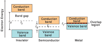
1. Energy Bands:
- Valence Band (VB):
- The highest energy band filled with electrons at absolute zero temperature.
- Electrons in this band are tightly bound to atoms.
- Conduction Band (CB):
- The next higher energy band where electrons are free to move.
- Electrons in this band can contribute to electrical conduction.
- Forbidden Energy Gap (Energy Band Gap):
- The energy range between the valence and conduction bands where no electron energy levels exist.
- Materials are classified as conductors, semiconductors, or insulators based on this gap.
2. Conductors, Semiconductors, and Insulators:
- Conductors:
- Have overlapping valence and conduction bands.
- Electrons are easily excited to the conduction band, contributing to high electrical conductivity.
- Semiconductors:
- Have a small energy gap between the valence and conduction bands.
- Electron transition to the conduction band is possible at higher temperatures, contributing to moderate electrical conductivity.
- Insulators:
- Have a large energy gap between the valence and conduction bands.
- Electrons require a significant amount of energy to move to the conduction band, resulting in low electrical conductivity.
3. Fermi Level:
- Definition:
- The energy level at which there is a 50% probability of finding an electron.
- At absolute zero, the Fermi level lies within the energy band gap.
- Effect of Temperature:
- As temperature increases, some electrons gain enough energy to move to the conduction band, contributing to electrical conduction.
4. Intrinsic and Extrinsic Semiconductors:
- Intrinsic Semiconductors:
- Pure semiconductors with no added impurities.
- Electron-hole pairs are created by thermal excitation.
- Extrinsic Semiconductors:
- Doped semiconductors with added impurities (dopants).
- N-type (donor) and P-type (acceptor) semiconductors are created, enhancing electrical conductivity.
Applications:
- Transistors:
- Utilize the behavior of semiconductors for amplification and switching in electronic devices.
- Integrated Circuits:
- Semiconductor materials form the basis of modern electronic components.
- Photovoltaic Cells:
- Exploit semiconductor properties to convert sunlight into electricity.
Conclusion:
Electron band theory provides a comprehensive understanding of how electrons behave in solid materials. It is crucial for explaining the diverse electrical and thermal properties observed in conductors, semiconductors, and insulators, forming the foundation for modern electronics and materials science.
EXPLANATION:-
In terms of electrical properties material can be defined into three groups conductor semiconductor and insulator on the basis of solid the distinction between metals semiconductor and insulator can be explained first it should be emphasized that empty energy bands with do not contain electrons do not contribute to the electrical conductivity of a material when as also completed bands contain electrons they do not contribute to the electrical conductivity since the carrier than unable to gain energy when the electric field is applied due to the fact that all the energy levels are occupied in comparison the partially filled and contain both electrons and occupied energy level in the presence of an applied electric field and can contribute to the electrical conductivity of the material in case of metals that electronic band structure results in incomplete filling of the highest occupied energy bank if an electron expires in a traditional energy from an external source it leaves the valence shell and becomes a free electron and exist in what is non the conduction band the difference in the net between the valid mad and the conduction band is called energy gap this is the amount of energy that a balance electron must have in order to jump from the balance bank to the conduction band the wellness band to the conduction band once in the conduction band the electron is free to move through out the material and its not tired any given item notice important insulator have a very wide energy gaps electrons cannot jump into the conduction band except under breakdown conditions where extremely high voltage are applied across the material in figure semiconductor have a much more energy gap this gap permit some balance electrons to jump into the conduction band and become free electron the energy bank in conductors of a lap has their large number of free electrons.
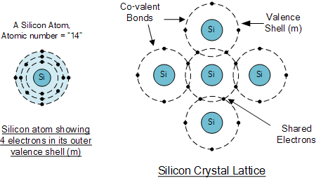
Silicon crystals :
silicon atoms combine to form solid they arrange themselves into an order pattern call krypton each silicon atom shares its electron with four neighbouring atoms in such a way as to have a electron in its balance orbit for instance show that a central atom with 4 neighbour item share and electron with the central atom in this way the central atom has 4 additional electrons giving it to the total of Airtel electrons in the Venus orbit the electrons no longer belong to any single item each central atom and its neighbour share electron the same idea is true for all other silicon atom in other words inside a silicon crystal has four neighbours since shade electron in figure directions the electrons become a bond between the opposite course this type of chemical bond is called covalent bond balance orbit these electrons produce chemical stability that results in a solid piece of silicon material when the balance of it has Airtel electrons it is saturated because no more electrons can fit into this in other word the balance orbit can hold no more than 8 electrons are silicon crystal perfect insulator at about 25 degree centigrade the ambit and temperature is the temperature of the surrounding air when the ambiton temperature is about absolute zero the heat energy in the air causes the atom in the silicon crystal to vibrate the higher the ambit and temperature the stronger than mechanical vibrations become in silicon crystal the vibrations of the atom casually does log an electron from the balance orbit when this happens the released electrons can give enough energy to go into larger orbits in the largest orbit the electron is a free electron the departure of the electron create a balance called this whole behave like a positive charge because the laws of electron produces a positive mind the whole will attain and capital and electron in the immediate visiting the existence of the critical difference between conductors and semiconductors to increase the number.
N-Type and P-Type Semiconductors:
In semiconductor physics, N-type (negative-type) and P-type (positive-type) refer to the two main types of extrinsic semiconductors, which are created by intentionally introducing impurities into the semiconductor material. These impurities, known as dopants, alter the conductivity and electronic properties of the semiconductor. Let’s explore the characteristics of N-type and P-type semiconductors:
N-Type Semiconductor:
- Doping:
- N-type semiconductors are doped with elements that have more electrons in their outer shell than the semiconductor material.
- Common dopants include phosphorus (P), arsenic (As), and antimony (Sb).
- Dopant Electron Behavior:
- Dopant atoms introduce extra electrons into the semiconductor crystal lattice.
- These extra electrons become the majority charge carriers.
- Electron Mobility:
- Electrons are mobile and contribute to electrical conductivity.
- N-type semiconductors have a higher electron concentration compared to intrinsic (undoped) semiconductors.
- Conduction Process:
- Electrons are the primary carriers of electric charge.
- When a voltage is applied, electrons move through the crystal lattice, contributing to current flow.
P-Type Semiconductor:
- Doping:
- P-type semiconductors are doped with elements that have fewer electrons in their outer shell than the semiconductor material.
- Common dopants include boron (B), aluminum (Al), and gallium (Ga).
- Dopant Hole Behavior:
- Dopant atoms create “holes” or vacant positions in the crystal lattice.
- These holes act as positive charge carriers.
- Hole Mobility:
- Holes move through the crystal lattice, contributing to electrical conductivity.
- P-type semiconductors have a higher hole concentration compared to intrinsic semiconductors.
- Conduction Process:
- Holes are the primary carriers of electric charge.
- When a voltage is applied, holes move through the crystal lattice, contributing to current flow.
Applications:
- N-Type:
- Commonly used in the fabrication of NPN transistors.
- Key component in the construction of electronic devices such as diodes and integrated circuits.
- P-Type:
- Integral in the manufacturing of PNP transistors.
- Essential for the development of electronic components like diodes and integrated circuits.
Conclusion:
N-type and P-type semiconductors play vital roles in the creation of electronic devices. The intentional introduction of dopants allows for the control of conductivity and the design of specific electronic components essential for modern technology. The combination of N-type and P-type semiconductors is foundational to the operation of transistors, diodes, and integrated circuits
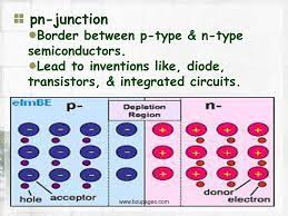
Formation of the Depletion Region
The free electrons in the n region are randomly drifting in all directions. At the instant of
the pn junction formation, the free electrons near the junction in the n region begin to diffuse across the junction into the p region where they combine with holes near the junction.
Before the pn junction is formed, recall that there are as many electrons as protons in
the n-type material, making the material neutral in terms of net charge. The same is true for
the p-type material.
When the pn junction is formed, the n region loses free electrons as they diffuse across
the junction. This creates a layer of positive charges (pentavalent ions) near the junction.
As the electrons move across the junction, the p region loses holes as the electrons and
holes combine. This creates a layer of negative charges (trivalent ions) near the junction.
These two layers of positive and negative charges form the depletion region,
. The term depletion refers to the fact that the region near the pn junction is
depleted of charge carriers (electrons and holes) due to diffusion across the junction. Keep
in mind that the depletion region is formed very quickly and is very thin compared to the n
region and p region.
After the initial surge of free electrons across the pn junction, the depletion region has
expanded to a point where equilibrium is established and there is no further diffusion of
electrons across the junction. This occurs as follows. As electrons continue to diffuse
across the junction, more and more positive and negative charges are created near the junction as the depletion region is formed. A point is reached where the total negative charge in
the depletion region repels any further diffusion of electrons (negatively charged particles)
into the p region (like charges repel) and the diffusion stops. In other words, the depletion
region acts as a barrier to the further movement of electrons across the junction.
Barrier Potential Any time there is a positive charge and a negative charge near each
other, there is a force acting on the charges as described by Coulomb’s law. In the depletion region there are many positive charges and many negative charges on opposite sides of the pn
junction. The forces between the opposite charges form an electric field, as illustrated in by the blue arrows between the positive charges and the negative charges. This
electric field is a barrier to the free electrons in the n region, and energy must be expended to
move an electron through the electric field. That is, external energy must be applied to get the
electrons to move across the barrier of the electric field in the depletion region.
The potential difference of the electric field across the depletion region is the amount of
voltage required to move electrons through the electric field. This potential difference is
called the barrier potential and is expressed in volts. Stated another way, a certain
amount of voltage equal to the barrier potential and with the proper polarity must be applied across a pn junction before electrons will begin to flow across the junction.
The barrier potential of a pn junction depends on several factors, including the type of
semiconductive material, the amount of doping, and the temperature. The typical barrier
potential is approximately 0.7 V for silicon and 0.3 V for germanium at Because germanium devices are not widely used, silicon will be used throughout the rest of the book.
")


 Assignment 1 Semester: Spring, 2024")
